Baseboard Ports
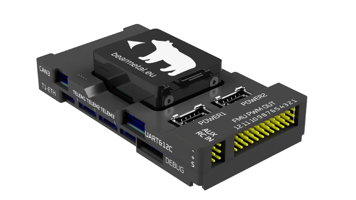
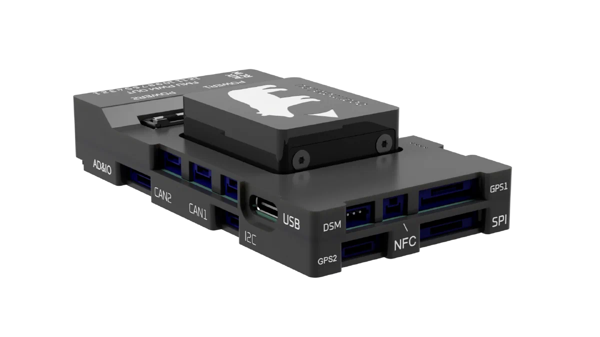
Directions are given from the board: TX (out) leaves the board, RX (in) enters it.
The 5 V on the ports comes from two rails, each with its own current limit. VDD_5V_HIPOWER feeds TELEM1 and GPS2; VDD_5V_PERIPH feeds TELEM2, TELEM3, CAN1, CAN2, CAN3, UART&I2C, GPS1, SPI, I2C, AD&IO.
In standard Pixhawk cables the pin 1 wire is red and the rest are black.
The 2.54 mm headers mark their rows −, + and S: top row A is GND (−), middle row B is power (+), bottom row C is the signal (S). Pins are numbered by position and row, so 3C is the signal pin of position 3.
Ports
| Ref | Port | Connector |
|---|---|---|
| J16 | POWER1 | Molex CLIK-Mate, 2.00 mm pitch, 6 pins |
| J17 | POWER2 | Molex CLIK-Mate, 2.00 mm pitch, 6 pins |
| J20 | FMU PWM OUT 1-8 | 2.54 mm right-angle header, 8 positions × 3 rows |
| J15 | FMU PWM OUT 9-12 | 2.54 mm right-angle header, 4 positions × 3 rows |
| J13 | RC IN / AUX | 2.54 mm right-angle header, 2 positions × 3 rows |
| J5 | TELEM1 | JST GH, 1.25 mm pitch, 6 pins |
| J3 | TELEM2 | JST GH, 1.25 mm pitch, 6 pins |
| J26 | TELEM3 | JST GH, 1.25 mm pitch, 6 pins |
| J9 | CAN1 | JST GH, 1.25 mm pitch, 4 pins |
| J10 | CAN2 | JST GH, 1.25 mm pitch, 4 pins |
| J6 | CAN3 | JST GH, 1.25 mm pitch, 4 pins |
| J21 | ETH | JST GH, 1.25 mm pitch, 2 pins |
| J8 | UART & I2C | JST GH, 1.25 mm pitch, 7 pins |
| J23 | FMU DEBUG | JST SH, 1.00 mm pitch, 10 pins |
| J18 | USB-C | Molex USB-C receptacle, right angle, 16 pins |
| J19 | USB | JST GH, 1.25 mm pitch, 4 pins |
| J4 | GPS1 | JST GH, 1.25 mm pitch, 10 pins |
| J7 | GPS2 | JST GH, 1.25 mm pitch, 6 pins |
| J11 | SPI | JST GH, 1.25 mm pitch, 11 pins |
| J2 | DSM RC | JST ZH, 1.50 mm pitch, 3 pins |
| J24 | I2C | JST GH, 1.25 mm pitch, 4 pins |
| J14 | AD & IO | JST GH, 1.25 mm pitch, 8 pins |
| J12 | NFC | JST GH, 1.25 mm pitch, 2 pins |
I2C buses
| Bus | Ports | Onboard devices |
|---|---|---|
| I2C1 | POWER1, GPS1 | |
| I2C2 | POWER2, GPS2 | |
| I2C6 | UART & I2C, I2C | 24LC64 EEPROM at 7-bit address 0x51, SE052 secure element address 0x48 |
Power, PWM output and RC input
POWER1 (J16), POWER2 (J17)
Molex CLIK-Mate, 2.00 mm pitch, 6 pins.
| Pin | Signal | Level |
|---|---|---|
| 1 | VDD5V | +5 V |
| 2 | VDD5V | +5 V |
| 3 | SCL | +3.3 V |
| 4 | SDA | +3.3 V |
| 5 | GND | GND |
| 6 | GND | GND |
Pins 3 and 4 connect the power module’s voltage and current monitor to the port’s I2C bus.
| Port | Role | I2C bus |
|---|---|---|
| POWER1 | main power input | I2C1 |
| POWER2 | backup power input | I2C2 |
FMU PWM OUT 1-8 (J20), 9-12 (J15)
2.54 mm right-angle header, 12 positions × 3 rows.
Positions are numbered 1 to 12 from right to left.
| Pin | Signal | Level |
|---|---|---|
| 1A to 12A (−) | GND | GND |
| 1B to 12B (+) | VDD_SERVO | external |
| 1C to 12C (S) | FMU_CH1 to FMU_CH12 | +3.3 V |
Pins 1-8 support DShot.
The board does not power VDD_SERVO; feed the rail from an external supply.
The VDD_SERVO voltage reading is only valid up to 9.9 V.
RC IN / AUX (J13)
2.54 mm right-angle header, 2 positions × 3 rows.
Position 1 is on the right, position 2 on the left.
| Pin | Signal | Level |
|---|---|---|
| 1A | − GND | GND |
| 1B | + VDD_5V_AUX | +5 V |
| 1C | S AUX out | +3.3 V |
| 2A | − GND | GND |
| 2B | + VDD_5V_RC | +5 V |
| 2C | S SBUS/PPM in | +3.3 V |
Connect the receiver to position 2. The input accepts SBUS or PPM.
Position 1 outputs SBUS, for a device that takes it.
Telemetry, network, serial and debug
TELEM1 (J5), TELEM2 (J3), TELEM3 (J26)
JST GH, 1.25 mm pitch, 6 pins.
| Pin | Signal | Level |
|---|---|---|
| 1 | VCC | +5 V |
| 2 | TX (out) | +3.3 V |
| 3 | RX (in) | +3.3 V |
| 4 | CTS (in) | +3.3 V |
| 5 | RTS (out) | +3.3 V |
| 6 | GND | GND |
All three support hardware flow control. TELEM1 shares its 5 V rail only with GPS2, so it is the port for the telemetry radio that draws the most current.
| Port | UART | Pin 1 rail |
|---|---|---|
| TELEM1 | UART4 | VDD_5V_HIPOWER |
| TELEM2 | UART8 | VDD_5V_PERIPH |
| TELEM3 | UART10 | VDD_5V_PERIPH |
CAN1 (J9), CAN2 (J10), CAN3 (J6)
JST GH, 1.25 mm pitch, 4 pins.
| Pin | Signal | Level |
|---|---|---|
| 1 | VCC (VDD_5V_PERIPH) | +5 V |
| 2 | CANH1 to CANH3 | +3.3 V |
| 3 | CANL1 to CANL3 | +3.3 V |
| 4 | GND | GND |
Three independent buses.
ETH (J21)
JST GH, 1.25 mm pitch, 2 pins.
| Pin | Signal | Level |
|---|---|---|
| 1 | TRX_P | differential |
| 2 | TRX_N | differential |
100BASE-T1. One twisted pair carries both directions, so there are no separate transmit and receive pins.
The PHY is strapped as master in autonomous mode, so the link partner must be the slave.
UART & I2C (J8)
JST GH, 1.25 mm pitch, 7 pins.
| Pin | Signal | Level |
|---|---|---|
| 1 | VCC (VDD_5V_PERIPH) | +5 V |
| 2 | TX (out) | +3.3 V |
| 3 | RX (in) | +3.3 V |
| 4 | SCL (I2C6) | +3.3 V |
| 5 | SDA (I2C6) | +3.3 V |
| 6 | NFC_GPIO | +3.3 V |
| 7 | GND | GND |
Labelled EXTERNAL 2 on the schematic. UART11 plus I2C6.
FMU DEBUG (J23)
JST SH, 1.00 mm pitch, 10 pins.
| Pin | Signal | Level |
|---|---|---|
| 1 | FMU_VDD_3V3 | +3.3 V |
| 2 | FMU_USART_TX | +3.3 V |
| 3 | FMU_USART_RX | +3.3 V |
| 4 | FMU_SWD_IO | +3.3 V |
| 5 | FMU_SWD_CK | +3.3 V |
| 6 | SPI6_MOSI | +3.3 V |
| 7 | NFC_GPIO | +3.3 V |
| 8 | GPIO_EMC_B2_12 | +3.3 V |
| 9 | FMU_nRST | +3.3 V |
| 10 | GND | GND |
Console and SWD debug probe.
USB-C (J18)
Molex USB-C receptacle, right angle, 16 pins.
| Pin | Signal | Level |
|---|---|---|
| A1 | GND | GND |
| A4 | VBUS | +5 V |
| A5 | CC1 | +3.3 V |
| A6 | DP | differential |
| A7 | DM | differential |
| A8 | SBU1 | not connected |
| A9 | VBUS | +5 V |
| A12 | GND | GND |
| B1 | GND | GND |
| B4 | VBUS | +5 V |
| B5 | CC2 | +3.3 V |
| B6 | DP | differential |
| B7 | DM | differential |
| B8 | SBU2 | not connected |
| B9 | VBUS | +5 V |
| B12 | GND | GND |
USB (J19)
JST GH, 1.25 mm pitch, 4 pins.
| Pin | Signal | Level |
|---|---|---|
| 1 | VBUS | +5 V |
| 2 | DM | differential |
| 3 | DP | differential |
| 4 | GND | GND |
The same USB signals as the USB-C receptacle, on a header beside it. Use one or the other, not both.
GNSS, SPI, RC, I2C and analogue IO
GPS1 (J4)
JST GH, 1.25 mm pitch, 10 pins.
| Pin | Signal | Level |
|---|---|---|
| 1 | VCC (VDD_5V_PERIPH) | +5 V |
| 2 | TX (out) | +3.3 V |
| 3 | RX (in) | +3.3 V |
| 4 | SCL (I2C1) | +3.3 V |
| 5 | SDA (I2C1) | +3.3 V |
| 6 | SAFETY_SWITCH | +3.3 V |
| 7 | SAFETY_SWITCH_LED | +3.3 V |
| 8 | VDD_3V3 | +3.3 V |
| 9 | BUZZER | 0 to 5 V |
| 10 | GND | GND |
UART3 and I2C1, plus the safety switch and the buzzer. This is the port for a GPS module with a compass and a safety switch with LED.
Wire the buzzer between pin 9 and a 5 V pin: pin 9 switches to GND to sound it.
GPS2 (J7)
JST GH, 1.25 mm pitch, 6 pins.
| Pin | Signal | Level |
|---|---|---|
| 1 | VCC (VDD_5V_HIPOWER) | +5 V |
| 2 | TX (out) | +3.3 V |
| 3 | RX (in) | +3.3 V |
| 4 | SCL (I2C2) | +3.3 V |
| 5 | SDA (I2C2) | +3.3 V |
| 6 | GND | GND |
UART5 and I2C2, for a second GPS module with a compass.
SPI (J11)
JST GH, 1.25 mm pitch, 11 pins.
| Pin | Signal | Level |
|---|---|---|
| 1 | VCC (VDD_5V_PERIPH) | +5 V |
| 2 | SPI_SCK | +3.3 V |
| 3 | SPI_MISO | +3.3 V |
| 4 | SPI_MOSI | +3.3 V |
| 5 | SPI_CS1 | +3.3 V |
| 6 | SPI_CS2 | +3.3 V |
| 7 | SPI_SYNC | +3.3 V |
| 8 | SPI_DRDY1 | +3.3 V |
| 9 | SPI_DRDY2 | +3.3 V |
| 10 | SPI_nRESET | +3.3 V |
| 11 | GND | GND |
External SPI sensors. Two chip selects, so two devices can share the port.
DSM RC (J2)
JST ZH, 1.50 mm pitch, 3 pins.
| Pin | Signal | Level |
|---|---|---|
| 1 | VDD_3V3_SPEKTRUM | +3.3 V |
| 2 | GND | GND |
| 3 | DSM/SPEKTRUM IN | +3.3 V |
Spektrum receiver, powered at 3.3 V.
This shares its input with position 2 of the RC IN / AUX header. Connect a receiver to either, never both.
I2C (J24)
JST GH, 1.25 mm pitch, 4 pins.
| Pin | Signal | Level |
|---|---|---|
| 1 | VCC (VDD_5V_PERIPH) | +5 V |
| 2 | SCL (I2C6) | +3.3 V |
| 3 | SDA (I2C6) | +3.3 V |
| 4 | GND | GND |
AD & IO (J14)
JST GH, 1.25 mm pitch, 8 pins.
| Pin | Signal | Level |
|---|---|---|
| 1 | VCC (VDD_5V_PERIPH) | +5 V |
| 2 | FMU_CAP | +3.3 V |
| 3 | FMU_BOOTLOADER | +3.3 V |
| 4 | FMU_RST_REQ | +3.3 V |
| 5 | NARMED | +3.3 V |
| 6 | ADC1_3V3 | 0 to 3.3 V |
| 7 | ADC1_6V6 | 0 to 6.6 V |
| 8 | GND | GND |
Analogue inputs and control lines. Pin 7 shares an ADC channel with the VDD_SERVO rail measurement; use one or the other.
NFC (J12)
JST GH, 1.25 mm pitch, 2 pins.
| Pin | Signal | Level |
|---|---|---|
| 1 | LB | coil |
| 2 | LA | coil |
NFC antenna coil for the onboard secure element.